Costo aproximado para acceder a varios cachés y memoria principal?
¿Puede alguien darme el tiempo aproximado (en nanosegundos) para acceder a las cachés L1, L2 y L3, así como a la memoria principal en los procesadores Intel i7?
Si bien esto no es específicamente una pregunta de programación, conocer este tipo de detalles de velocidad es necesario para algunos desafíos de programación de baja latencia.
EDIT:
El segundo enlace de Dave servía los siguientes números:
Core i7 Xeon 5500 Series Data Source Latency (approximate)               [Pg. 22]

local  L1 CACHE hit,                              ~4 cycles (   2.1 -  1.2 ns )
local  L2 CACHE hit,                             ~10 cycles (   5.3 -  3.0 ns )
local  L3 CACHE hit, line unshared               ~40 cycles (  21.4 - 12.0 ns )
local  L3 CACHE hit, shared line in another core ~65 cycles (  34.8 - 19.5 ns )
local  L3 CACHE hit, modified in another core    ~75 cycles (  40.2 - 22.5 ns )

remote L3 CACHE (Ref: Fig.1 [Pg. 5])        ~100-300 cycles ( 160.7 - 30.0 ns )

local  DRAM                                                   ~60 ns
remote DRAM                                                  ~100 ns
EDIT2:
El más importante es el aviso debajo de la tabla citada, diciendo:
"NOTA: ESTOS VALORES SON APROXIMACIONES APROXIMADAS. DEPENDEN DE FRECUENCIAS CORE Y UNCORE, VELOCIDADES DE MEMORIA, AJUSTES DEL BIOS, NÚMEROS DE DIMM , ETC, ETC..SU KILOMETRAJE PUEDE VARIAR."
5 answers
Aquí hay una Guía de Análisis de rendimiento para la gama de procesadores i7 y Xeon. Debo enfatizar, esto tiene lo que necesita y más (por ejemplo, consulte la página 22 para ver algunos tiempos y ciclos, por ejemplo).
Además, esta página tiene algunos detalles sobre los ciclos de reloj, etc
EDITAR: Debo resaltar que, además de la información de tiempo/ciclo, el documento de intel anterior aborda detalles mucho más (extremadamente) útiles de la gama de procesadores i7 y Xeon (desde rendimiento punto de vista).
Warning: date(): Invalid date.timezone value 'Europe/Kyiv', we selected the timezone 'UTC' for now. in /var/www/agent_stack/data/www/ajaxhispano.com/template/agent.layouts/content.php on line 61
2010-11-03 13:31:10
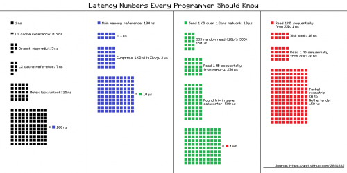
Números que todo el mundo debería saber
           0.5 ns - CPU L1 dCACHE reference
           1   ns - speed-of-light (a photon) travel a 1 ft (30.5cm) distance
           5   ns - CPU L1 iCACHE Branch mispredict
           7   ns - CPU L2  CACHE reference
          71   ns - CPU cross-QPI/NUMA best  case on XEON E5-46*
         100   ns - MUTEX lock/unlock
         100   ns - own DDR MEMORY reference
         135   ns - CPU cross-QPI/NUMA best  case on XEON E7-*
         202   ns - CPU cross-QPI/NUMA worst case on XEON E7-*
         325   ns - CPU cross-QPI/NUMA worst case on XEON E5-46*
      10,000   ns - Compress 1K bytes with Zippy PROCESS
      20,000   ns - Send 2K bytes over 1 Gbps NETWORK
     250,000   ns - Read 1 MB sequentially from MEMORY
     500,000   ns - Round trip within a same DataCenter
  10,000,000   ns - DISK seek
  10,000,000   ns - Read 1 MB sequentially from NETWORK
  30,000,000   ns - Read 1 MB sequentially from DISK
 150,000,000   ns - Send a NETWORK packet CA -> Netherlands
|   |   |   |
|   |   | ns|
|   | us|
| ms|
Desde:
Original de Peter Norvig:
- http://norvig.com/21-days.html#answers
- http://surana.wordpress.com/2009/01/01/numbers-everyone-should-know/,
- http://sites.google.com/site/io/building-scalable-web-applications-with-google-app-engine
Warning: date(): Invalid date.timezone value 'Europe/Kyiv', we selected the timezone 'UTC' for now. in /var/www/agent_stack/data/www/ajaxhispano.com/template/agent.layouts/content.php on line 61
2017-05-13 13:43:02
Costo para acceder a varios recuerdos en una página bonita
Resumen
-
Los valores han disminuido pero se han estabilizado desde 2005
1 ns L1 cache 3 ns Branch mispredict 4 ns L2 cache 17 ns Mutex lock/unlock 100 ns Main memory (RAM) 2 000 ns (2µs) 1KB Zippy-compress -
Todavía algunas mejoras, predicción para 2020
   16 000 ns (16µs) SSD random read (olibre's note: should be less)
  500 000 ns (½ms)  Round trip in datacenter
2 000 000 ns (2ms)  HDD random read (seek)
Ver también otras fuentes
-
Lo que todo programador debe saber sobre la memoria de Ulrich Drepper (2007)
Viejo pero sigue siendo una excelente explicación profunda sobre la interacción de hardware y software de memoria.- PDF completo (114 páginas)
- Siete publicaciones en LWN + Comentarios
- Post El Espacio Infinito Entre Palabras en codinghorror.com basado en book Rendimiento de los sistemas: la Empresa y la nube
- Haga clic en cada procesador listado en http://www.7-cpu.com / para ver el L1/L2/L3/RAM/... latencias (e. g. Haswell i7-4770 has L1=1ns, L2=3ns, L3=10ns, RAM=67ns, BranchMisprediction=4ns)
- http://idarkside.org/posts/numbers-you-should-know /
Véase también una formación
Para una mayor comprensión, recomiendo la excelente presentación de arquitecturas de caché modernas (junio de 2014) de Gerhard Wellein, Hannes Hofmann and Dietmar Fey at University Erlangen-Nürnberg.
Warning: date(): Invalid date.timezone value 'Europe/Kyiv', we selected the timezone 'UTC' for now. in /var/www/agent_stack/data/www/ajaxhispano.com/template/agent.layouts/content.php on line 61
2015-10-13 08:00:59
Solo por el bien de la revisión de 2015 de las predicciones para 2020:
Still some improvements, prediction for 2020 (Ref. olibre's answer below)
-------------------------------------------------------------------------
   16 000 ns ( 16 µs) SSD random read (olibre's note: should be less)
  500 000 ns (  ½ ms) Round trip in datacenter
2 000 000 ns (  2 ms) HDD random read (seek)

In 2015 there are currently available:
========================================================================
      820 ns ( 0.8µs)     random read from a SSD-DataPlane
    1 200 ns ( 1.2µs) Round trip in datacenter
    1 200 ns ( 1.2µs)     random read from a HDD-DataPlane
Solo por el bien de la CPU y GPU latencia paisaje comparación:
No es una tarea fácil comparar incluso las alineaciones de CPU / caché / DRAM más simples ( incluso en un modelo de acceso a memoria uniforme), donde la velocidad de DRAM es un factor para determinar la latencia, y la latencia cargada (sistema saturado), donde este último gobierna y es algo que las aplicaciones empresariales experimentarán más que sistema.
                    +----------------------------------- 5,6,7,8,9,..12,15,16
                    |                               +--- 1066,1333,..2800..3300
                    v                               v
First  word = ( ( CAS latency * 2 ) + ( 1 - 1 ) ) / Data Rate
Fourth word = ( ( CAS latency * 2 ) + ( 4 - 1 ) ) / Data Rate
Eighth word = ( ( CAS latency * 2 ) + ( 8 - 1 ) ) / Data Rate
                                        ^----------------------- 7x .. difference
********************************
So:
===

resulting DDR3-side latencies are between _____________
                                          3.03 ns    ^
                                                     |
                                         36.58 ns ___v_ based on DDR3 HW facts
Los motores de GPU han recibido mucho marketing técnico, mientras que las dependencias internas profundas son claves para comprender tanto las fortalezas reales como las debilidades reales que estas arquitecturas experimentan en la práctica ( generalmente muy diferentes de las expectativas de marketing agresivo ).
   1 ns _________ LETS SETUP A TIME/DISTANCE SCALE FIRST:
          °      ^
          |\     |a 1 ft-distance a foton travels in vacuum ( less in dark-fibre )
          | \    |
          |  \   |
        __|___\__v____________________________________________________
          |    |
          |<-->|  a 1 ns TimeDOMAIN "distance", before a foton arrived
          |    |
          ^    v
    DATA  |    |DATA
    RQST'd|    |RECV'd ( DATA XFER/FETCH latency )

  25 ns @ 1147 MHz FERMI:  GPU Streaming Multiprocessor REGISTER access
  35 ns @ 1147 MHz FERMI:  GPU Streaming Multiprocessor    L1-onHit-[--8kB]CACHE

  70 ns @ 1147 MHz FERMI:  GPU Streaming Multiprocessor SHARED-MEM access

 230 ns @ 1147 MHz FERMI:  GPU Streaming Multiprocessor texL1-onHit-[--5kB]CACHE
 320 ns @ 1147 MHz FERMI:  GPU Streaming Multiprocessor texL2-onHit-[256kB]CACHE

 350 ns
 700 ns @ 1147 MHz FERMI:  GPU Streaming Multiprocessor GLOBAL-MEM access
 - - - - -
Comprender los internalidades es, por lo tanto, mucho más importante que en otros campos, donde las arquitecturas son publicadas y numerosas benchmarks disponibles gratuitamente. Muchas gracias a GPU-micro-probadores, que ' he pasado su tiempo y creatividad para dar rienda suelta a la verdad de los esquemas reales de trabajo dentro de la caja negra enfoque probado dispositivos GPU.
    +====================| + 11-12 [usec] XFER-LATENCY-up   HostToDevice    ~~~ same as Intel X48 / nForce 790i
    |   |||||||||||||||||| + 10-11 [usec] XFER-LATENCY-down DeviceToHost
    |   |||||||||||||||||| ~  5.5 GB/sec XFER-BW-up                         ~~~ same as DDR2/DDR3 throughput
    |   |||||||||||||||||| ~  5.2 GB/sec XFER-BW-down @8192 KB TEST-LOAD      ( immune to attempts to OverClock PCIe_BUS_CLK 100-105-110-115 [MHz] ) [D:4.9.3]
    |
    |              Host-side
    |                                                        cudaHostRegister(   void *ptr, size_t size, unsigned int flags )
    |                                                                                                                 | +-------------- cudaHostRegisterPortable -- marks memory as PINNED MEMORY for all CUDA Contexts, not just the one, current, when the allocation was performed
    |                        ___HostAllocWriteCombined_MEM / cudaHostFree()                                           +---------------- cudaHostRegisterMapped   -- maps  memory allocation into the CUDA address space ( the Device pointer can be obtained by a call to cudaHostGetDevicePointer( void **pDevice, void *pHost, unsigned int flags=0 ); )
    |                        ___HostRegisterPORTABLE___MEM / cudaHostUnregister( void *ptr )
    |   ||||||||||||||||||
    |   ||||||||||||||||||
    |   | PCIe-2.0 ( 4x) | ~ 4 GB/s over  4-Lanes ( PORT #2  )
    |   | PCIe-2.0 ( 8x) | ~16 GB/s over  8-Lanes
    |   | PCIe-2.0 (16x) | ~32 GB/s over 16-Lanes ( mode 16x )
    |
    |   + PCIe-3.0 25-port 97-lanes non-blocking SwitchFabric ... +over copper/fiber
    |                                                                       ~~~ The latest PCIe specification, Gen 3, runs at 8Gbps per serial lane, enabling a 48-lane switch to handle a whopping 96 GBytes/sec. of full duplex peer to peer traffic. [I:]
    |
    | ~810 [ns]    + InRam-"Network" / many-to-many parallel CPU/Memory "message" passing with less than 810 ns latency any-to-any
    |
    |   ||||||||||||||||||
    |   ||||||||||||||||||
    +====================|
    |.pci............HOST|
Mi disculpa por una "imagen más grande", pero latencia-demasking también tiene límites cardinales impuestos desde en el chip smREG/L1/L2-capacidades y hit/miss-tasas.
|.pci............GPU.|
| | FERMI [GPU-CLK] ~ 0.9 [ns] but THE I/O LATENCIES PAR -- ||||||||||||||||||||||||||||||||||||||||||||||||||||||||||||||||||||||||||| <800> warps ~~ 24000 + 3200 threads ~~ 27200 threads [!!]
| ^^^^^^^^|~~~~~~~~~~~~~~~~~~~~~~~~~~~~~~~~~~~~~~~~~~~~~~~~~~~~~~~~~~~~~~~~~~~~~~~~~~~~~~~~~~~~~~~~~~~~~~~~~~~~~~~~~~~~~~~~~~~~~~~ [!!]
| smREGs________________________________________ penalty +400 ~ +800 [GPU_CLKs] latency ( maskable by 400~800 WARPs ) on <Compile-time>-designed spillover(s) to locMEM__
| +350 ~ +700 [ns] @1147 MHz FERMI ^^^^^^^^
| | ^^^^^^^^
| +5 [ns] @ 200 MHz FPGA. . . . . . Xilinx/Zync Z7020/FPGA massive-parallel streamline-computing mode ev. PicoBlazer softCPU
| | ^^^^^^^^
| ~ +20 [ns] @1147 MHz FERMI ^^^^^^^^
| SM-REGISTERs/thread: max 63 for CC-2.x -with only about +22 [GPU_CLKs] latency ( maskable by 22-WARPs ) to hide on [REGISTER DEPENDENCY] when arithmetic result is to be served from previous [INSTR] [G]:10.4, Page-46
| max 63 for CC-3.0 - about +11 [GPU_CLKs] latency ( maskable by 44-WARPs ) [B]:5.2.3, Page-73
| max 128 for CC-1.x PAR -- ||||||||~~~|
| max 255 for CC-3.5 PAR -- ||||||||||||||||||~~~~~~|
|
| smREGs___BW ANALYZE REAL USE-PATTERNs IN PTX-creation PHASE << -Xptxas -v || nvcc -maxrregcount ( w|w/o spillover(s) )
| with about 8.0 TB/s BW [C:Pg.46]
| 1.3 TB/s BW shaMEM___ 4B * 32banks * 15 SMs * half 1.4GHz = 1.3 TB/s only on FERMI
| 0.1 TB/s BW gloMEM___
| ________________________________________________________________________________________________________________________________________________________________________________________________________________________
+========| DEVICE:3 PERSISTENT gloMEM___
| _|______________________________________________________________________________________________________________________________________________________________________________________________________________________
+======| DEVICE:2 PERSISTENT gloMEM___
| _|______________________________________________________________________________________________________________________________________________________________________________________________________________________
+====| DEVICE:1 PERSISTENT gloMEM___
| _|______________________________________________________________________________________________________________________________________________________________________________________________________________________
+==| DEVICE:0 PERSISTENT gloMEM_____________________________________________________________________+440 [GPU_CLKs]_________________________________________________________________________|_GB|
! | |\ + |
o | texMEM___|_\___________________________________texMEM______________________+_______________________________________________________________________________________|_MB|
| |\ \ |\ + |\ |
| texL2cache_| \ \ .| \_ _ _ _ _ _ _ _texL2cache +370 [GPU_CLKs] _ _ _ _ _ _ _ _ _ _ _ _ _ _ _ _ | \ 256_KB|
| | \ \ | \ + |\ ^ \ |
| | \ \ | \ + | \ ^ \ |
| | \ \ | \ + | \ ^ \ |
| texL1cache_| \ \ .| \_ _ _ _ _ _texL1cache +260 [GPU_CLKs] _ _ _ _ _ _ _ _ _ | \_ _ _ _ _^ \ 5_KB|
| | \ \ | \ + ^\ ^ \ ^\ \ |
| shaMEM + conL3cache_| \ \ | \ _ _ _ _ conL3cache +220 [GPU_CLKs] ^ \ ^ \ ^ \ \ 32_KB|
| | \ \ | \ ^\ + ^ \ ^ \ ^ \ \ |
| | \ \ | \ ^ \ + ^ \ ^ \ ^ \ \ |
| ______________________|__________\_\_______________________|__________\_____^__\________+__________________________________________\_________\_____\________________________________|
| +220 [GPU-CLKs]_| |_ _ _ ___|\ \ \_ _ _ _ _ _ _ _ _ _ _ _ _ _ _ _ _ \ _ _ _ _\_ _ _ _+220 [GPU_CLKs] on re-use at some +50 GPU_CLKs _IF_ a FETCH from yet-in-shaL2cache
| L2-on-re-use-only +80 [GPU-CLKs]_| 64 KB L2_|_ _ _ __|\\ \ \_ _ _ _ _ _ _ _ _ _ _ _ _ _ _ _ _ \ _ _ _ _\_ _ _ + 80 [GPU_CLKs] on re-use from L1-cached (HIT) _IF_ a FETCH from yet-in-shaL1cache
| L1-on-re-use-only +40 [GPU-CLKs]_| 8 KB L1_|_ _ _ _|\\\ \_\__________________________________\________\_____+ 40 [GPU_CLKs]_____________________________________________________________________________|
| L1-on-re-use-only + 8 [GPU-CLKs]_| 2 KB L1_|__________|\\\\__________\_\__________________________________\________\____+ 8 [GPU_CLKs]_________________________________________________________conL1cache 2_KB|
| on-chip|smREG +22 [GPU-CLKs]_| |t[0_______^:~~~~~~~~~~~~~~~~\:________]
|CC- MAX |_|_|_|_|_|_|_|_|_|_|_| |t[1_______^ :________]
|2.x 63 |_|_|_|_|_|_|_|_|_|_|_| |t[2_______^ :________]
|1.x 128 |_|_|_|_|_|_|_|_|_|_|_| |t[3_______^ :________]
|3.5 255 REGISTERs|_|_|_|_|_|_|_|_| |t[4_______^ :________]
| per|_|_|_|_|_|_|_|_|_|_|_| |t[5_______^ :________]
| Thread_|_|_|_|_|_|_|_|_|_| |t[6_______^ :________]
| |_|_|_|_|_|_|_|_|_|_|_| |t[7_______^ 1stHalf-WARP :________]______________
| |_|_|_|_|_|_|_|_|_|_|_| |t[ 8_______^:~~~~~~~~~~~~~~~~~:________]
| |_|_|_|_|_|_|_|_|_|_|_| |t[ 9_______^ :________]
| |_|_|_|_|_|_|_|_|_|_|_| |t[ A_______^ :________]
| |_|_|_|_|_|_|_|_|_|_|_| |t[ B_______^ :________]
| |_|_|_|_|_|_|_|_|_|_|_| |t[ C_______^ :________]
| |_|_|_|_|_|_|_|_|_|_|_| |t[ D_______^ :________]
| |_|_|_|_|_|_|_|_|_|_|_| |t[ E_______^ :________]
| |_|_|_|_|_|_|_|_|_|_|_| W0..|t[ F_______^____________WARP__:________]_____________
| |_|_|_|_|_|_|_|_|_|_|_| ..............
| |_|_|_|_|_|_|_|_|_|_|_| ............|t[0_______^:~~~~~~~~~~~~~~~\:________]
| |_|_|_|_|_|_|_|_|_|_|_| ............|t[1_______^ :________]
| |_|_|_|_|_|_|_|_|_|_|_| ............|t[2_______^ :________]
| |_|_|_|_|_|_|_|_|_|_|_| ............|t[3_______^ :________]
| |_|_|_|_|_|_|_|_|_|_|_| ............|t[4_______^ :________]
| |_|_|_|_|_|_|_|_|_|_|_| ............|t[5_______^ :________]
| |_|_|_|_|_|_|_|_|_|_|_| ............|t[6_______^ :________]
| |_|_|_|_|_|_|_|_|_|_|_| ............|t[7_______^ 1stHalf-WARP :________]______________
| |_|_|_|_|_|_|_|_|_|_|_| ............|t[ 8_______^:~~~~~~~~~~~~~~~~:________]
| |_|_|_|_|_|_|_|_|_|_|_| ............|t[ 9_______^ :________]
| |_|_|_|_|_|_|_|_|_|_|_| ............|t[ A_______^ :________]
| |_|_|_|_|_|_|_|_|_|_|_| ............|t[ B_______^ :________]
| |_|_|_|_|_|_|_|_|_|_|_| ............|t[ C_______^ :________]
| |_|_|_|_|_|_|_|_|_|_|_| ............|t[ D_______^ :________]
| |_|_|_|_|_|_|_|_|_|_|_| ............|t[ E_______^ :________]
| |_|_|_|_|_|_|_|_|_|_|_| W1..............|t[ F_______^___________WARP__:________]_____________
| |_|_|_|_|_|_|_|_|_|_|_| ....................................................
| |_|_|_|_|_|_|_|_|_|_|_| ...................................................|t[0_______^:~~~~~~~~~~~~~~~\:________]
| |_|_|_|_|_|_|_|_|_|_|_| ...................................................|t[1_______^ :________]
| |_|_|_|_|_|_|_|_|_|_|_| ...................................................|t[2_______^ :________]
| |_|_|_|_|_|_|_|_|_|_|_| ...................................................|t[3_______^ :________]
| |_|_|_|_|_|_|_|_|_|_|_| ...................................................|t[4_______^ :________]
| |_|_|_|_|_|_|_|_|_|_|_| ...................................................|t[5_______^ :________]
| |_|_|_|_|_|_|_|_|_|_|_| ...................................................|t[6_______^ :________]
| |_|_|_|_|_|_|_|_|_|_|_| ...................................................|t[7_______^ 1stHalf-WARP :________]______________
| |_|_|_|_|_|_|_|_|_|_|_| ...................................................|t[ 8_______^:~~~~~~~~~~~~~~~~:________]
| |_|_|_|_|_|_|_|_|_|_|_| ...................................................|t[ 9_______^ :________]
| |_|_|_|_|_|_|_|_|_|_|_| ...................................................|t[ A_______^ :________]
| |_|_|_|_|_|_|_|_|_|_|_| ...................................................|t[ B_______^ :________]
| |_|_|_|_|_|_|_|_|_|_|_| ...................................................|t[ C_______^ :________]
| |_|_|_|_|_|_|_|_|_|_|_| ...................................................|t[ D_______^ :________]
| |_|_|_|_|_|_|_|_|_|_|_| ...................................................|t[ E_______^ :________]
| |_|_|_|_|_|_|_|_|_|_|_|tBlock Wn....................................................|t[ F_______^___________WARP__:________]_____________
|
| ________________ °°°°°°°°°°°°°°°°°°°°°°°°°°~~~~~~~~~~°°°°°°°°°°°°°°°°°°°°°°°°°°°°°°°°°°°°°°°°°°°°°°°°°°°°°°°°°°°°°°°°°°°°°°°°°°
| / \ CC-2.0|||||||||||||||||||||||||| ~masked ||||||||||||||||||||||||||||||||||||||||||||||||||||||||||||||||||||||||||
| / \ 1.hW ^|^|^|^|^|^|^|^|^|^|^|^|^| <wait>-s ^|^|^|^|^|^|^|^|^|^|^|^|^|^|^|^|^|^|^|^|^|^|^|^|^|^|^|^|^|^|^|^|^|^|^|^|^|
| / \ 2.hW |^|^|^|^|^|^|^|^|^|^|^|^|^ |^|^|^|^|^|^|^|^|^|^|^|^|^|^|^|^|^|^|^|^|^|^|^|^|^|^|^|^|^|^|^|^|^|^|^|^|^
|_______________/ \______I|I|I|I|I|I|I|I|I|I|I|I|I|~~~~~~~~~~I|I|I|I|I|I|I|I|I|I|I|I|I|I|I|I|I|I|I|I|I|I|I|I|I|I|I|I|I|I|I|I|I|I|I|I|I|
|~~~~~~~~~~~~~~/ SM:0.warpScheduler /~~~~~~~I~I~I~I~I~I~I~I~I~I~I~I~I~~~~~~~~~~~I~I~I~I~I~I~I~I~I~I~I~I~I~I~I~I~I~I~I~I~I~I~I~I~I~I~I~I~I~I~I~I~I~I~I~I~I
| \ | //
| \ RR-mode //
| \ GREEDY-mode //
| \________________//
| \______________/SM:0__________________________________________________________________________________
| | |t[ F_______^___________WARP__:________]_______
| ..|SM:1__________________________________________________________________________________
| | |t[ F_______^___________WARP__:________]_______
| ..|SM:2__________________________________________________________________________________
| | |t[ F_______^___________WARP__:________]_______
| ..|SM:3__________________________________________________________________________________
| | |t[ F_______^___________WARP__:________]_______
| ..|SM:4__________________________________________________________________________________
| | |t[ F_______^___________WARP__:________]_______
| ..|SM:5__________________________________________________________________________________
| | |t[ F_______^___________WARP__:________]_______
| ..|SM:6__________________________________________________________________________________
| | |t[ F_______^___________WARP__:________]_______
| ..|SM:7__________________________________________________________________________________
| | |t[ F_______^___________WARP__:________]_______
| ..|SM:8__________________________________________________________________________________
| | |t[ F_______^___________WARP__:________]_______
| ..|SM:9__________________________________________________________________________________
| ..|SM:A |t[ F_______^___________WARP__:________]_______
| ..|SM:B |t[ F_______^___________WARP__:________]_______
| ..|SM:C |t[ F_______^___________WARP__:________]_______
| ..|SM:D |t[ F_______^___________WARP__:________]_______
| |_______________________________________________________________________________________
*/
La línea de fondo?
Cualquier diseño motivado de baja latencia tiene que realice ingeniería inversa de la" hidráulica de E/S " (ya que 0 1-XFERs son incompresibles por naturaleza ) y las latencias resultantes gobiernan la envolvente de rendimiento para cualquier solución GPGPU, ya sea computacionalmente intensiva ( léase: donde los costos de procesamiento perdonan un poco más a los XFERs de latencia pobre ... ) o no ( read : donde ( podría sorprender a alguien ) las CPU-s son más rápidas en el procesamiento de extremo a extremo que las telas de GPU [citas disponibles]).
Warning: date(): Invalid date.timezone value 'Europe/Kyiv', we selected the timezone 'UTC' for now. in /var/www/agent_stack/data/www/ajaxhispano.com/template/agent.layouts/content.php on line 61
2017-06-05 00:11:01
Mira esta trama de "escalera", que ilustra perfectamente los diferentes tiempos de acceso (en términos de tics de reloj). Observe que la CPU roja tiene un "paso" adicional, probablemente porque tiene L4 (mientras que otros no).
Gráficos de tiempos de acceso con diferentes jerarquías de memoria
Tomado de este artículo de Extremetech.
En informática esto se llama "complejidad de E/S".
Warning: date(): Invalid date.timezone value 'Europe/Kyiv', we selected the timezone 'UTC' for now. in /var/www/agent_stack/data/www/ajaxhispano.com/template/agent.layouts/content.php on line 61
2018-04-01 21:27:33